Design Principles and Practical Guide for Optocoupler-Isolated Relay Protection Circuits
In industrial automation, smart home systems, and various power electronics applications, relays frequently serve as the core actuating components for controlling high-power loads. However, the back-electromotive force (back-EMF) generated when the relay coil is de-energized, combined with high-frequency noise from the high-voltage side, can easily feed back into the low-voltage control circuitry via conduction or radiation. This can cause control chips to reset or freeze, or even result in permanent hardware damage.
To achieve safe physical isolation between the low-voltage control system and the high-voltage load, the use of an architecture combining optocoupler isolation, relay driving, and back-EMF suppression has become a standard practice in industrial circuit design. This article systematically outlines the design principles, key component selection, and PCB layout considerations for optocoupler-isolated relay protection circuits.
I. Core Protection Mechanisms of Optocoupler-Isolated Relay Circuits
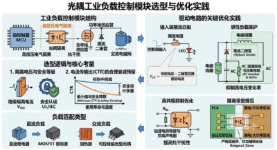
A complete optocoupler-isolated relay circuit consists of four core modules: the low-voltage control signal interface, the optocoupler isolation module, the relay driving and protection module, and the high-voltage load interface. Its protection mechanism operates across two dimensions:
Physical and Electrical Isolation
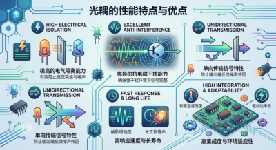
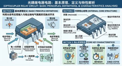
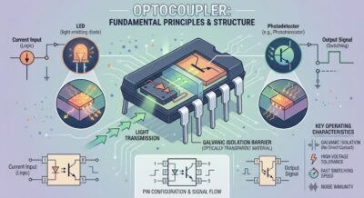
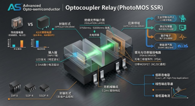
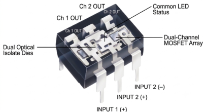
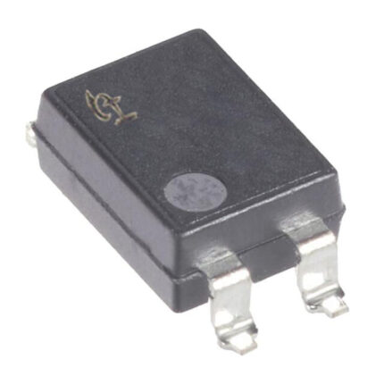
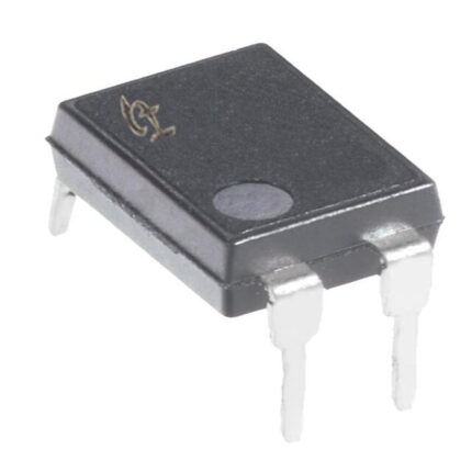
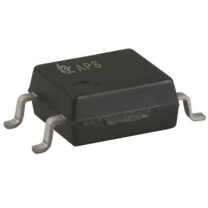
Optocouplers utilize light as the transmission medium. When input current is applied to the control side, the internal light-emitting diode (LED) emits light, causing the photosensitive transistor on the receiving side to conduct. The low-voltage control side and the high-voltage driving side are electrically completely decoupled, with no direct conductive path between them. This structure not only withstands isolation voltages of several kilovolts but also completely eliminates ground loop interference, preventing noise from the high-voltage side from affecting the control system’s ground reference point.
Flyback Protection and Energy Dissipation
The relay’s internal control coil is essentially an inductive component. The moment the driving transistor or MOSFET cuts off the current, the coil current drops abruptly to zero, inducing a high-amplitude voltage spike of opposite polarity across the coil terminals. Without suppression, this high voltage would cause immediate breakdown of the driving transistor. Connecting a flyback diode or a transient voltage suppression (TVS) diode in reverse-parallel across the coil terminals provides a discharge path for the coil’s stored energy, thereby protecting the driving components.
II. Design and Principle Analysis of Key Circuit Modules
Control Input and Optocoupler Current Limiting
The control input is typically driven by a microcontroller port. When the control signal is active, the internal light-emitting diode (LED) of the optocoupler turns on. To ensure the LED operates within a safe and stable current range, a current-limiting resistor must be connected in series at the input. Insufficient current slows down the optocoupler’s response, while excessive current accelerates the degradation of the LED’s light output. The resistor value should be calculated based on the input voltage and the LED’s forward voltage drop.
Matching the Optocoupler (Isolation Side) with the Driver Stage
The Current Transfer Ratio (CTR)—defined as the ratio of the output collector current to the input LED current—is a critical design parameter. Since CTR is affected by ambient temperature and component aging, calculations should be based on the minimum rated transfer ratio (derating). Because the output side of an optocoupler typically cannot supply enough current to directly drive a relay coil requiring high operating current, a secondary power amplification stage—such as a low-power transistor or a MOSFET—must be added.
Driver Component and State Determination
Taking transistor-based relay driving as an example: to ensure the transistor operates reliably in a state of deep saturation, the base current must meet minimum drive requirements while maintaining sufficient margin. Additionally, a pull-down resistor should be connected in parallel between the driver transistor’s control terminal and ground. This resistor pulls the control terminal potential low during system power-up or when the control signal is floating, preventing the driver transistor from malfunctioning due to external interference while in a high-impedance state.
III. Selection of Key Protection Components for the Relay Protection Circuit
The protection circuit on the relay coil side is crucial for ensuring the long-term operational stability of the entire system. Flyback Diode
A flyback diode is connected in anti-parallel across the relay coil terminals, with its cathode connected to the positive power supply rail and its anode to the switching terminal of the driver transistor. When the driver transistor cuts off, the back electromotive force (back-EMF) induced by the coil circulates through the diode, forming a closed loop that dissipates electromagnetic energy as heat.
Voltage and Current Ratings: The diode’s reverse breakdown voltage rating should significantly exceed the relay’s operating voltage, and its rated forward current should be equal to or greater than the relay coil’s rated operating current.
Type Selection: General-purpose rectifier diodes are suitable for standard low-frequency switching applications; however, if the relay operates frequently or requires precise release timing, fast-recovery diodes or Schottky diodes are recommended.
Advanced Voltage Clamping and Snubber Circuits
Relying solely on a flyback diode can prolong the relay contact release time, thereby accelerating contact erosion caused by arcing. If high response speed is required, the following alternative or supplementary solutions may be employed:
Transient Voltage Suppressor (TVS) Diode: Connected in series with the flyback diode or directly in parallel, it clamps high reverse voltages to a safe level, significantly accelerating the dissipation of coil energy.
RC Snubber Circuit: A network consisting of a resistor and a capacitor connected in parallel across the coil or driver transistor to absorb high-frequency voltage spikes.
Arc Suppression for High-Power Contacts
Relay contacts generate arcs when switching heavy loads, leading to contact erosion and intense electromagnetic interference. For AC loads, an RC snubber or varistor can be connected in parallel across the contacts; for DC inductive loads (such as DC motors or solenoid valves), a flyback diode must be connected in anti-parallel across the load itself. IV. PCB Layout and Grounding Specifications for Interference Immunity
Even with a flawless circuit schematic, an incorrect PCB layout can still lead to isolation failure or system instability.
Ground Isolation and Slotting
Low-voltage control grounds and high-voltage drive grounds must never be directly connected on the PCB. Optocouplers should bridge the isolation zone separating the low-voltage and high-voltage sections. All copper layers beneath the optocoupler must be cleared away. For applications requiring strict high-voltage isolation, a physical slot should be cut into the PCB between the two rows of optocoupler pins to prevent surface creepage.
Loop Minimization and Decoupling
Flyback diodes must be placed immediately adjacent to the relay coil pins. The area enclosed by the current loop—formed by the relay coil, flyback diode, and driver transistor—should be minimized to reduce high-frequency electromagnetic interference (EMI) radiation. Additionally, decoupling capacitors must be placed close to the power input to absorb current surges generated when the relay engages.
V. Conclusion
The design of optocoupler-isolated relay protection circuits encompasses signal isolation, current matching, inductive load overvoltage suppression, and electromagnetic compatibility (EMC). By adhering to fundamental principles—such as physical isolation, parameter matching, protection against back-EMF, and close placement of flyback components—and by combining rigorous component selection and calculation with proper PCB isolation layouts, one can create industrial-grade control systems that are stable, reliable, and highly resistant to interference.
This concludes the article. If you found this content helpful, please continue to follow our website (https://www.a-semi.com) and our WeChat official account, “先进光半导体” (Advanced Opto-Semiconductor), for more news, information, and technical insights. Copyright Notice: Some articles and information are sourced from the internet or user submissions. This website is responsible only for the organization, formatting, and editing of the content. These materials are published to share information and do not imply endorsement of the views expressed or verification of the content’s accuracy. If any articles or submitted content raise copyright or related issues, authors are requested to contact us promptly so that we may address the matter as soon as possible.