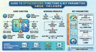
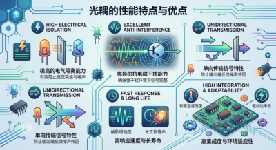
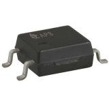
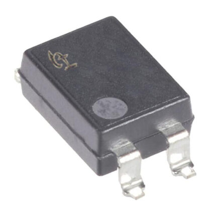
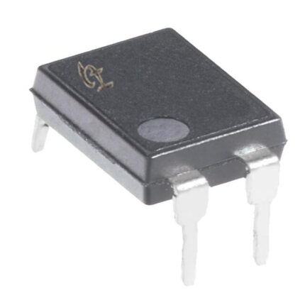
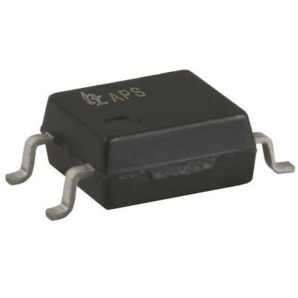
In the design of isolation circuits and high-reliability electronic systems—such as switching power supplies, automotive electronics, and industrial automation controls—optocouplers (or optoisolators) are critical components for signal isolation and transmission. Among the key performance parameters of an optocoupler, the Current Transfer Ratio (CTR) is undoubtedly one of the most crucial metrics.
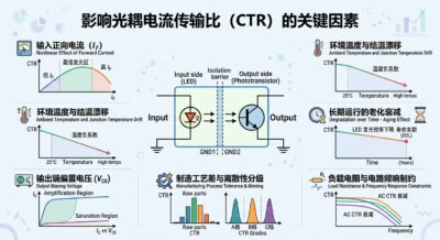
CTR is defined as the ratio of the output collector current to the input LED forward drive current, typically expressed as a percentage. Ideally, designers would prefer CTR to be a constant value; however, in practical applications, CTR exhibits significant nonlinearity and dynamic drift characteristics. If engineers overlook CTR fluctuations when designing feedback loops or signal transmission paths, it can easily lead to signal distortion, sluggish response, or even system failure after prolonged operation or exposure to high temperatures. To achieve highly stable circuit designs, it is essential to thoroughly understand and master the six key factors that influence an optocoupler’s CTR.
1. Nonlinear effects of the input forward drive current
The input forward current is the most direct parameter determining the CTR, and the relationship between the two is nonlinear rather than a simple linear correspondence.
In the low-current range—where the input current is very small—the internal luminous efficiency of the light-emitting diode (LED) drops significantly due to recombination mechanisms, resulting in an insufficient number of emitted photons. Consequently, the phototransistor absorbs very limited light energy, causing the output current to be disproportionately low and the CTR to remain at a low level.
As the input current increases into the device’s typical operating range (usually between a few milliamperes and over ten milliamperes), the LED’s luminous efficiency peaks and the phototransistor operates in its optimal gain region, causing the CTR to rise to its maximum value. However, as the input current continues to increase and approaches saturation, the LED’s luminous efficiency declines due to heating and hot-carrier effects. Simultaneously, the output phototransistor enters the saturation region or a high-injection state, causing a significant drop in current gain; ultimately, the CTR value decreases as the input current becomes excessive. Therefore, biasing the input current within the optimal plateau region of the CTR curve is crucial for ensuring efficient signal transmission.
II. Ambient Temperature and Junction Temperature Drift
An optocoupler consists of a light-emitting diode (LED) and a photodetector. Both semiconductor components are highly temperature-sensitive, collectively causing the CTR to exhibit a distinct negative temperature coefficient.
First, the LED’s quantum efficiency decreases as temperature rises. When the ambient temperature or the chip’s junction temperature increases, the luminous flux emitted by the LED drops significantly for a given drive current.
Second, although the phototransistor’s current gain may increase slightly with rising temperature, this is insufficient to compensate for the loss caused by the sharp decline in the LED’s light output.
The combined effect is that, at temperatures above 25°C, the CTR value degrades to varying degrees as the temperature rises. In high-temperature industrial environments (such as 85°C to 125°C), the CTR value may drop to 50%–70% of its room-temperature level. Designers must account for this high-temperature degradation factor when calculating loop gain margins.
III. LED Luminous Efficiency Degradation During Long-Term Operation
After prolonged continuous operation, an optocoupler’s CTR value inevitably declines over time—a phenomenon known as optocoupler aging.
The root cause of this aging lies in the physical degradation of the input LED material: prolonged exposure to current stress and thermal stress creates lattice defects in the LED’s light-emitting junction region. This leads to an increase in non-radiative recombination centers, causing the LED’s luminous efficiency to decrease progressively over time. The two primary factors influencing aging are the magnitude of the average drive current and the operating junction temperature. For optocouplers operated for extended periods at extreme currents or high temperatures, the rate of CTR (Current Transfer Ratio) degradation accelerates exponentially. For products requiring long-term reliable operation (5 to 10 years), engineering designs must perform worst-case calculations based on the minimum CTR expected at the end of the component’s service life (typically derated to 50%–80% of the initial CTR).
IV. Output-Side Bias Voltage and Operating State
The collector-emitter voltage of the output phototransistor directly determines its operating state (active/amplification region or saturation region), which in turn profoundly affects the measured CTR value.
In the linear amplification region, when the collector-emitter voltage is relatively high (e.g., above 5V) and the device has not entered saturation, the phototransistor exhibits high collector responsivity; the measured CTR is higher and more accurately reflects the device’s electrical-to-optical-to-electrical conversion capability.
In the deep saturation region, when the collector current is limited by an external load resistor—causing the collector-emitter voltage to drop to the saturation voltage level (e.g., 0.2V to 0.4V)—the phototransistor’s amplification capability is suppressed, and the actual output collector current is far lower than the theoretical value for the amplification region. The apparent CTR calculated in this state drops significantly. When comparing parameters or performing circuit calculations, it is essential to verify the voltage conditions under which the cited CTR specifications were measured.
V. Manufacturing Process Variations and Binning
During optocoupler production, minor variations—such as the uniformity of the LED epitaxial wafer, control of phototransistor doping concentrations, and alignment precision during the encapsulation of the internal optical coupling medium—result in a wide distribution of CTR values among units from the same production batch.
For general-purpose optocouplers (such as the PC817 series), the overall CTR distribution range can span from 50% to 600% if the devices are not sorted into specific grades (binned). To meet the varying gain consistency requirements of different circuits, manufacturers typically grade components based on CTR ranges (e.g., Grade A: 80%–160%; Grade B: 130%–260%; Grade C: 200%–400%). Selecting the wrong grade during circuit design can lead to imbalances in loop control.
VI. Constraints Imposed by Load Resistance and Circuit Frequency Response
Although load resistance does not alter the optocoupler’s internal physical gain, it indirectly affects the effective CTR in the actual circuit by influencing the output voltage drop and response speed.
A high load resistance can easily cause the output transistor to pull the output voltage low and enter saturation even with minimal drive current, thereby prematurely limiting the observed CTR. Furthermore, the load resistance and the phototransistor’s junction capacitance form a low-pass filter. In high-speed signal transmission, an excessive or mismatched load limits the system’s dynamic response, resulting in significant attenuation of the AC CTR at high frequencies.
In summary, the Current Transfer Ratio (CTR) of an optocoupler is by no means a static nominal value; rather, it is a dynamic variable influenced by drive current, ambient temperature, operating time (aging), bias voltage, manufacturing process variations, and external load resistance. High-quality electronic engineering designs should employ a “worst-case” design approach to ensure sufficient gain margin, establish appropriate drive current ranges, and prioritize the use of high-performance optocouplers with clearly defined grading, thereby guaranteeing system stability and reliability throughout its entire lifecycle.
That concludes this article. If you found this information helpful, please continue to follow our website (https://www.a-semi.com) and our WeChat official account, “Advanced Opto-Semiconductor” (先进光半导体), for more news, updates, and educational content.
Copyright Notice: Some information in this article is sourced from the internet and user submissions. This website is responsible only for the organization, formatting, and editing of the content. These materials are shared to disseminate information and do not necessarily reflect our endorsement of the views expressed or the accuracy of the content. If any articles or submissions involve copyright issues, please contact us promptly so we can address the matter.