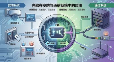
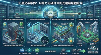
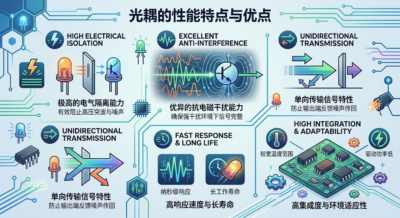
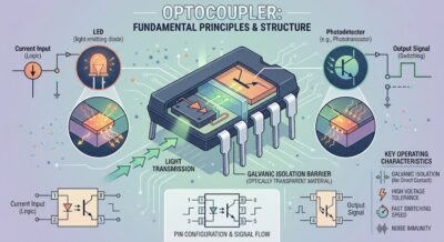
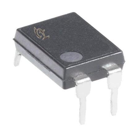
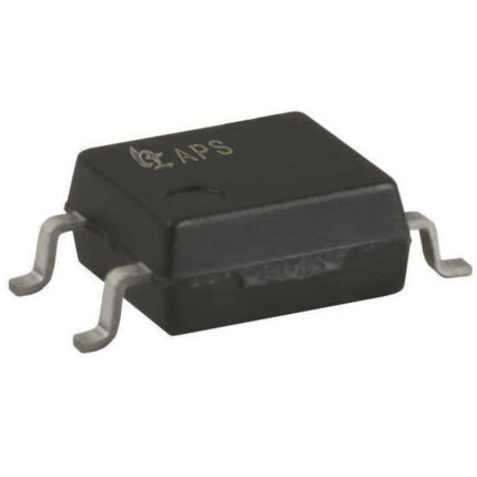
In modern electronic circuit design, signal isolation and transmission are crucial for ensuring system stability and safety. Optocouplers, abbreviated as optos, are widely used in industrial control, switching power supplies, medical equipment, communication systems, automotive electronics, and other fields due to their excellent electrical isolation capabilities, good anti-interference characteristics, and compact size. However, faced with a wide range of opto products on the market, how can one scientifically and accurately select the right type? What are the details that cannot be ignored during the selection process? This article will comprehensively break down the core elements and considerations for opto selection for you.
1. Clarify application scenarios and optocoupler classification
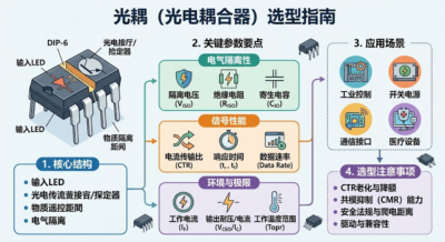
The first step in optocoupler selection is to determine the required type of optocoupler based on the needs of the actual circuit. Different application scenarios have distinct focuses on the performance requirements of optocouplers:
Transistor output type optocoupler: The most common basic optocoupler, suitable for general low-frequency switch control, signal isolation, and low-speed data transmission.
High-speed optocoupler: It integrates a high-speed photoelectric detection chip internally, with a response speed of up to several megahertz or even tens of megahertz. It is commonly used for pulse signal isolation, communication interfaces (such as serial ports, buses), and high-speed transmission of digital signals.
Thyristor output optocoupler: specifically designed for driving and controlling AC loads, capable of directly triggering bidirectional thyristors to achieve safe isolation between strong and weak electrical currents.
Linear optocoupler: It has good input-output linearity and can accurately transmit analog signals, commonly used in precision sampling and feedback loops for voltage or current.
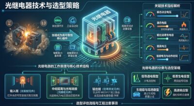
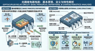
Optocoupler relay (PhotoMOS/SSR): Utilizing the technology of photo-driven MOSFET, it features no mechanical contacts, no noise, long lifespan, and low on-resistance, making it suitable for high-density contact control and micro-signal switching.
II. Key points for core parameter selection
After determining the general category of optocouplers, it is necessary to conduct refined selection by comparing specific technical parameters.
1. Electrical isolation performance parameters
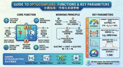
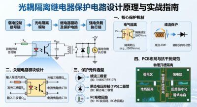
Isolation voltage: Refers to the maximum voltage difference that can be withstood between the input and output terminals of an optocoupler. Typically, industrial and power supply applications require isolation voltages of several thousand volts or more. When selecting a model, the isolation voltage specification must exceed the rated value of the system design safety standard, with sufficient safety margin reserved.
Insulation resistance and parasitic capacitance: High insulation resistance can prevent small leakage currents from interfering with sensitive circuits; while lower input and output parasitic capacitance helps to suppress the penetration of high-frequency common-mode interference.
2. Signal transmission and conversion efficiency parameters
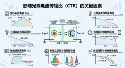
Current Transfer Ratio (CTR): This is one of the most critical parameters of an optocoupler, representing the ratio of the output current to the operating current of the input light-emitting diode (LED). CTR is not a fixed constant; it varies with changes in input current, ambient temperature, and usage duration. When selecting an optocoupler, it is important not to rely solely on the maximum or typical values, but rather to focus on evaluating the minimum values within the operating current range and at extreme temperatures. If CTR is too low, it may result in insufficient driving capability; if CTR is too high, it is prone to noise interference and false triggering at low input currents.
Response time and data rate: This includes rise time, fall time, turn-on delay, and turn-off delay. For high-frequency pulses or high-speed data communication signals, it is necessary to choose high-speed optocouplers with response times in the nanosecond range to ensure that the signal waveform is not distorted or delayed.
3. Operating limits and environmental parameters
Input forward current: The current required for a light-emitting diode (LED) to emit light normally. When selecting an LED, it is necessary to ensure that the preceding driver circuit can provide a stable operating current, while not exceeding the maximum rated current of the optocoupler, in order to avoid accelerating the aging of the light-emitting device.
Output voltage withstand and maximum current: The maximum collector voltage and current that the output transistor or MOSFET can withstand. During design, it is necessary to ensure that the actual operating voltage and current on the output side are below these limit values to prevent breakdown and burnout.
Operating temperature range: The operating environments of electronic devices vary greatly. Industrial-grade devices typically require optocouplers capable of withstanding temperature changes ranging from minus 40 degrees Celsius to 85 degrees Celsius or even higher. As the temperature rises, the luminous efficiency of light-emitting diodes (LEDs) decreases, leading to a reduction in CTR. Therefore, when selecting components, derating design must be implemented to account for performance degradation at high temperatures.
III. Key considerations in optocoupler selection
In practical engineering applications, merely meeting theoretical parameter specifications is insufficient. It is also necessary to consider engineering details to avoid potential hazards:
1. Pay attention to the performance degradation and lifespan of optocouplers
As the operating time increases, the luminous efficiency of the light-emitting diode inside the optocoupler will gradually decrease, a phenomenon known as aging of the light-emitting device. Aging can lead to a decline in the current transfer ratio (CTR) of the optocoupler over time. Therefore, when selecting the CTR and designing the input drive current, appropriate redundancy must be reserved to ensure that the optocoupler can operate stably throughout the entire product design lifecycle.
2. Emphasize common mode rejection (CMR) capability
In industrial sites or environments with strong electromagnetic interference, high-steep voltage transitions can generate common-mode interference currents on the parasitic capacitance between the optocoupler’s input and output, leading to signal mis-triggering. Optocouplers with high common-mode rejection ratio (CMR) feature a special shielding structure internally, effectively resisting such high-frequency interference and ensuring the accuracy of signal transmission.
3. Strictly consider the creepage distance and electrical clearance
For electrical safety and certification requirements, the physical package size of optocouplers is equally important. In high-voltage isolation applications, it is necessary to check whether the creepage distance and electrical clearance of the optocoupler package comply with industry safety standards (such as safety certification specifications). For high voltage difference isolation requirements, optocoupler devices with wide-body packages should be preferred.
4. Evaluate logical compatibility and drive capability
For digital optocouplers or high-speed optocouplers, it is important to ensure that their output logic levels match the subsequent microcontroller or signal processing chip. Additionally, the drive current required at the input should align with the load capacity of the preceding logic gate circuit. If necessary, preceding drive transistors or buffers should be added.
IV. Summary and Selection Suggestions
Optocoupler selection is a systematic process that comprehensively considers electrical isolation, signal performance, environmental tolerance, service life, and physical packaging. In summary, the selection can follow a “three-step method”:
Step 1: Determine the general category of optocoupler based on the circuit function type (such as switch, high-frequency, analog quantity, high-voltage trigger, etc.);
Step 2: Based on the system’s rated voltage, transmission rate, operating current, and temperature range, verify core parameters such as isolation voltage, current transfer ratio (CTR), and response time;
Step 3: Comprehensively consider anti-interference requirements, long-term aging redundancy, and physical safety standards to ensure the long-term reliability of the design.
Scientific and reasonable selection of optocouplers can not only effectively isolate high voltage and noise interference, ensuring the safety of subsequent core chips, but also significantly enhance the stability and service life of the entire electronic system. In practical design, leaving sufficient design margin based on specific application scenarios is the golden rule for creating high-quality electronic products.
That concludes the entire content of this article. If you find this article helpful, please stay tuned to our website https://www.a-semi.com and the official account of “APSEMI” on WeChat. We will bring you more news and informative content!
Copyright Notice: Some article information is sourced from the internet and submissions from netizens. This website is solely responsible for organizing, typesetting, and editing the articles. It aims to disseminate more information and does not imply endorsement of the views expressed or verification of the authenticity of the content. If the articles and reprints on this site involve copyright issues, please contact us promptly, and we will address them as soon as possible.