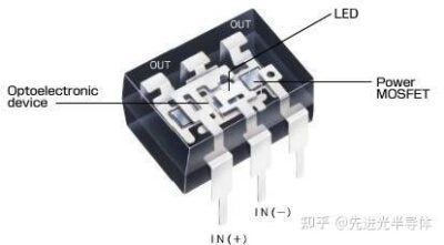
1) First, clarify the objects: two types of “optical relay drive” architectures
The commonly used “optical relay drive circuits” in engineering can be roughly divided into two categories:
Optocoupler isolation+transistor/MOSFET driver+mechanical relay coil: The optocoupler is responsible for isolation, the downstream power device is responsible for providing coil current, and the mechanical contacts are responsible for switching loads. The advantages are low cost and wide applicability; Shortcomings are prominent in terms of contact life and arc issues.
Direct switching load of optical MOS relay/solid-state relay (SSR): internally driven by optocoupler MOSFET/bidirectional device to achieve contactless switching. The advantages are no mechanical wear, anti vibration, and long service life; Shortboard is more sensitive to conduction voltage drop/leakage current, surge capability, and heat dissipation design.
The first step in reliability design is to confirm whether you are facing “coil drive reliability” or “solid-state switch reliability”, because the weak points of the two are completely different: the former often fails in contact and coil transients, while the latter often fails in heat and surges.
2) Reliability of optoelectronic isolation devices: CTR/trigger current margin is the core
Both optocouplers and optical MOS/SSR rely on LED illumination on the input side. The long-term aging of LED will bring two direct consequences:
The CTR of the optocoupler decreases: The current available on the output side of the optocoupler decreases, resulting in insufficient driving in the subsequent stage.
Therefore, reliability design must adhere to three principles:
Design based on worst-case parameters: Use the minimum CTR (or maximum trigger current, minimum output capacity) in the data manual for calculation, rather than typical values.
Consider temperature drift and aging: high temperatures can accelerate LED decay and also alter output side characteristics; When designing, “high temperature+end of life” should be considered as the worst-case scenario.
The input current should be “sufficient but not excessive”: too low a current will fail after aging, while too high a current will accelerate aging and increase heat generation. A more reliable approach is to increase the gain and protection of the rear stage driver within a reasonable range of LED current, rather than simply pulling up the LED current.
3) Driver level reliability: avoiding chain failures of “inability to drive – heating – even more inability to drive”
In the scheme of “optocoupler+power transistor+coil”, the most common hidden dangers are: insufficient optocoupler output current or temperature drift leading to power transistor undersaturation and insufficient enhancement of MOSFET, resulting in increased power consumption, junction temperature, and ultimately accelerated aging or even breakdown. This type of problem often “occasionally occurs” in the laboratory, but it will erupt in a concentrated manner during high temperatures or power fluctuations on site.
The key points of reliability design include:
Drive margin: Ensure that the power transistor can still meet the coil current requirements and maintain a low loss working area under the worst CTR, lowest power supply, and highest temperature.
Derating of power devices: Adequate margins should be left for current, withstand voltage, and power consumption, especially for spikes at the moment when the coil is turned off, which can increase device stress.
Thermal design: For continuous suction or high duty cycle applications, device junction temperature must be evaluated; If necessary, increase copper foil heat dissipation, thermal vias, or select lower loss devices.
4) Coil and back electromotive force: Turning off transient determines’ how long it can last ‘
Relay coils are typical inductive loads that generate back electromotive force spikes when turned off. If there is a lack of suitable clamping, the peak will impact the power tube and optocoupler output side, causing hidden damage, manifested as “sudden failure after a period of use”.
Common suppression strategies and reliability trade-offs:
Freewheeling diode (DC coil): the simplest and most reliable, capable of significantly reducing spikes; The cost is slower release, which may affect system response or result in longer contact arcing time.
Diode+Zener/TVS clamp: While protecting the device, increase the clamp voltage to make the coil demagnetize faster and release faster; Suitable for scenarios that are sensitive to release time.
RC absorption/TVS (AC coil or special drive): Depending on the driving method, the key is to provide a “controllable outlet” for peak energy.
Reliability design is not as simple as “with or without diodes”, but rather depends on the action time EMI、 Choose the appropriate clamping method based on the voltage resistance and lifespan goals of the device.
5) Contact and load: The lifespan of mechanical relays is often determined by the load
If it is ultimately the mechanical contacts that switch the load, the upper limit of the system’s lifespan is usually determined by contact arcing and material migration. The type of load has a significant impact on reliability:
Resistive loads are relatively friendly, but attention should still be paid to surges (such as cold current in incandescent lamps).
When the inductive load (motor, solenoid valve) is disconnected, the arc is strong, and the risk of contact erosion and adhesion is high.
Capacitive loads (switching power supply input, large capacitors) have large closing surges and are prone to welding contacts.
Reliability design recommendations:
The selection of relays should depend on the load category curve and surge capacity, not just the rated current.
RC absorption is commonly used for AC inductive loads, and MOV/TVS or pre charging/NTC schemes can be used for surges.
If the switching frequency is high or the environmental vibration is large, priority should be given to replacing mechanical contacts with optical MOS/SSR.
6) Power integrity and anti-interference: solving “occasional misoperation” and “jitter”
The common faults on site are not “completely inactive”, but “occasional suction, shaking, false triggering, MCU reset”. The root cause often comes from power and ground circuits:
The sudden change in current at the moment of coil attraction caused a power drop, and the logic power supply was dragged down.
Coil reflux and logical coupling cause ground bounce, leading to false triggering.
The EMI generated by the contact arc is coupled to the input end through the wiring harness.
Key points of reliability design:
Place electrolysis and ceramic decoupling near the coil power supply end, and plan a short and thick return path.
Logically separate from power ground and use a single point connection to avoid coil current passing through sensitive ground.
Add current limiting, filtering, and surge protection to external interfaces, and perform common mode suppression if necessary.
7) PCB isolation and environment: Creepage distance, pollution, and humidity can cause “chronic breakdown”
The voltage resistance of the optoelectronic isolation device itself does not necessarily mean that the system is safe. Moisture, dust, and residual flux can reduce insulation performance, leading to leakage, misoperation, and even breakdown. Reliability design should focus on:
The creepage distance/electrical clearance between the high and low voltage sides meets the standards and application environment.
If necessary, slotting, adding insulation isolation tape or three proof paint.
Connectors and wiring harnesses should also meet the isolation level to avoid “qualified on board but wiring harness failure”.
8) Verification and Mass Production Consistency: Implementing Reliability through Testing
Reliability is not guaranteed by experience, but by verifying closed loops. It is recommended to cover at least:
Measurement of suction/conduction margin of the worst parameter sample (low CTR/high trigger current) at high and low temperatures
Coil shutdown peak and EMI testing to verify clamping scheme
Life and surge testing under representative loads (inductive/capacitive)
Power drop, misoperation and reset testing under EFT/ESD anti-interference
At the same time, mass production should pay attention to optocoupler CTR grading, relay batch differences, welding processes, and cleanliness, all of which will consume the “design margin”.
Conclusion: The reliability design of the optical relay drive circuit is essentially about “being able to operate stably under the worst conditions and directing inevitable energy (coil recoil, load surge, arc EMI) to a controllable path”. Only by firmly grasping the five things of CTR aging, driving margin, transient suppression, load characteristics, and power supply and PCB isolation, can the circuit move from “usable” to “durable”.
The above is the entire content of this article. If you find it helpful, please continue to follow our website https://www.a-semi.com As well as “Advanced Optical Semiconductor” WeChat official account, we will bring you more news and knowledge!
Copyright Notice: Some article information is sourced from the internet and submissions from netizens. This website is only responsible for organizing, formatting, and editing the articles for the purpose of conveying more information, and does not imply endorsement of their views or confirmation of the authenticity of their content. If there are any copyright issues related to articles or submissions on this website, please contact us promptly and we will handle them as soon as possible.