In modern electronic system design, signal isolation and power control between high- and low-voltage circuits are critical for ensuring the safe and stable operation of equipment. While traditional mechanical relays once dominated the field of electrical control due to their straightforward contact-based switching mechanisms, the evolution of electronic devices toward miniaturization, high-frequency operation, low power consumption, and extended service life has exposed the inherent limitations of mechanical contacts—such as susceptibility to wear, arcing, slow response times, and operational noise—turning them into technical bottlenecks. Against this backdrop, optocoupler relays (also known as PhotoMOS SSRs)—which combine optocoupling principles with semiconductor MOSFET technology—have emerged. As a specialized domestic manufacturer in the fields of opto-isolation and power devices, Advanced Opto-semiconductor offers optocoupler relays that deliver significant technical advantages—including the absence of mechanical contacts, high insulation isolation, exceptional longevity, and superior electromagnetic compatibility—making them ideal for applications in industrial control, test and measurement, medical electronics, and new energy vehicles.
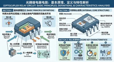
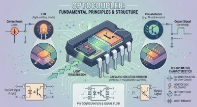
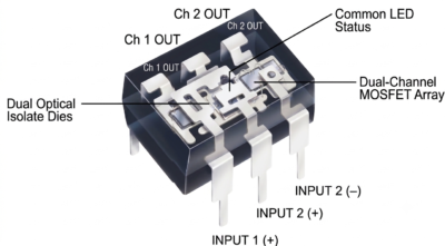
An optocoupler relay is essentially a solid-state electronic switch that utilizes light as the transmission medium. The internal architecture of Advanced Opto-semiconductor’s optocoupler relays comprises three core components: a light-emitting element at the input, an insulating optical transmission medium in the center, and a light-receiving and power-driving circuit at the output. During operation, when a low-level control current is applied to the input, a high-efficiency light-emitting diode (LED) emits light at a specific wavelength. This optical signal passes through an optical transmission layer—characterized by high insulation and voltage-withstand capabilities—and strikes the light-receiving chip at the output stage. A photodiode array (PDA) integrated into the receiving chip captures the optical energy and converts it into electrical energy, generating a high-voltage drive signal that activates back-to-back connected power MOSFETs, thereby closing the output circuit. When the input current is cut off, the LED ceases emission, the photodiode array discharges the gate charge, the MOSFETs turn off, and the output reverts to a high-impedance, open-circuit state. This control mechanism, based entirely on photoelectric conversion, eliminates physical contacts and achieves true “contactless” switching. Compared to traditional mechanical relays and standard transistor-output optocouplers, Advanced Opto-Semiconductor’s optocoupler relays achieve multi-dimensional breakthroughs in overall performance. First, they offer an exceptionally long service life and high reliability. With no internal mechanical parts prone to wear, these relays are immune to issues such as contact wear, metal oxidation, contact sticking, or mechanical fatigue; their theoretical switching cycle count is virtually unlimited, drastically reducing long-term equipment maintenance costs. Second, they deliver superior switching speeds. While mechanical relays typically have response times ranging from several to over ten milliseconds, Advanced Opto-Semiconductor’s optocoupler relays feature turn-on and turn-off times in the sub-millisecond or even microsecond range, easily meeting the demands of high-frequency switching and precise timing control.
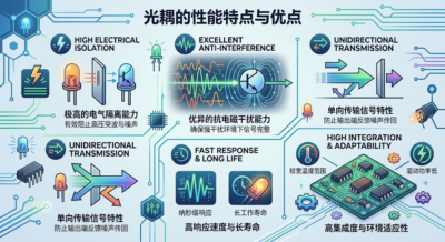
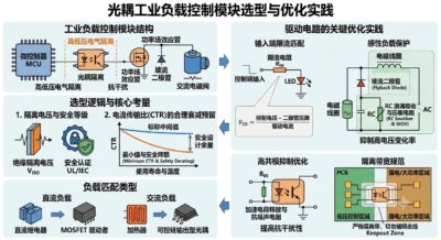
Regarding power consumption and drive characteristics, these optocoupler relays demonstrate outstanding energy efficiency. They can be reliably triggered by a tiny input current of just a few milliamperes—or even less—allowing for direct control via microcontrollers (MCUs), digital logic gates, or PLC GPIO interfaces without complex intermediate driver circuitry. This not only simplifies system circuit design but also significantly lowers the device’s overall standby power consumption. On the output side, the use of a back-to-back MOSFET structure enables excellent AC/DC versatility, allowing the relays to control both DC and AC loads with high linearity, minimal distortion, and extremely low leakage current. Furthermore, as the switching process generates no electrical sparks or electromagnetic interference, these relays are ideally suited for use in flammable or explosive environments and in high-precision measurement equipment that is highly sensitive to noise.
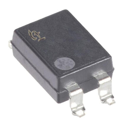
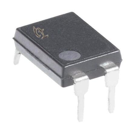
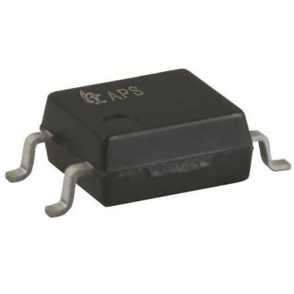
To meet the diverse parameter and mounting requirements of customers across various industries, Advanced Opto-Semiconductor has established an extensive product portfolio. In terms of isolation voltage, the products generally offer input-to-output isolation capabilities ranging from 3750 Vrms to 5000 Vrms, effectively withstanding high-voltage surges and transient spikes common in industrial settings while ensuring the safety of personnel and equipment on the low-voltage control side. Regarding on-resistance and current-carrying capacity, optimization of MOSFET chip processes has enabled some low-impedance models to achieve on-resistance levels in the milliohm range; this effectively reduces heat generation during high-current operation and enhances thermal management efficiency. For high-frequency applications such as Automated Test Equipment (ATE), Advanced Opto-Semiconductor has developed a Low-Output Capacitance (Low-COFF) series. This series significantly minimizes signal leakage and high-frequency attenuation in the off-state, thereby ensuring the integrity of high-frequency test signals. The product lineup encompasses various package types—including DIP, SOP, SSOP, and miniaturized leadless packages—which save significant PCB mounting space and accommodate the increasingly compact designs of modern circuit boards.
In practical applications, Advanced Opto-Semiconductor’s opto-relays have been widely adopted across critical industrial sectors. In industrial automation and PLC systems, they serve as isolation interfaces for digital I/O modules, isolating noise interference from field sensors, solenoid valves, and motors to ensure the stable operation of control cores. In test and measurement equipment, these opto-relays are key components in high-density signal switching matrices, data acquisition cards, and battery testing channels. In the new energy and Battery Management System (BMS) sectors, their high isolation voltage capabilities are utilized for high-voltage sampling, insulation monitoring, and safety circuit switching. In medical equipment—such as patient monitors and electrocardiographs—the opto-relays provide a reliable electrical safety barrier for patients and healthcare personnel, thanks to their low leakage current and high safety isolation ratings.
In summary, driven by continuous investment in optoelectronic isolation technology and process optimization, Advanced Opto-Semiconductor’s opto-relay products excel in electrical isolation, switching performance, reliability, and power consumption control. As industries accelerate their transition toward intelligence and electrification—and as requirements for safety isolation and noise-free control in equipment become increasingly stringent—Advanced Opto-Semiconductor’s opto-relays will continue to serve as core components, delivering stable, efficient, and safe isolation control solutions for industrial and electronic systems. That concludes this article. If you found it helpful, please continue to follow our website (https://www.a-semi.com) and our WeChat official account, “先进光半导体” (Advanced Optical Semiconductor), for more news and educational content.
Copyright Notice: Some content in our articles is sourced from the internet or user submissions. This website is responsible only for the compilation, formatting, and editing of the material; publication is intended solely to share information and does not imply endorsement of the views expressed or verification of the content’s accuracy. If any articles or submitted content raise copyright or related issues, please contact us promptly so we can address the matter.