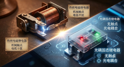
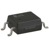
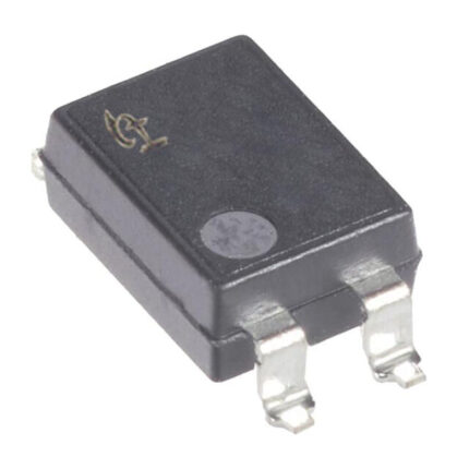
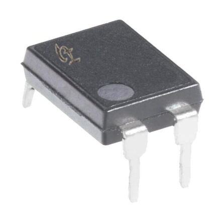
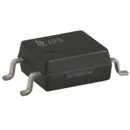
With the rapid evolution of new energy vehicles, industrial automation, intelligent computing servers, and high-precision test and measurement equipment, system performance requirements for signal control and power switching have reached unprecedented levels. Traditional mechanical relays, due to their physical contacts, face engineering bottlenecks such as limited lifespan, bulky size, slow response times, and contact bounce. Against this backdrop, solid-state switches based on optocoupling principles—specifically optical relays (or Photo-MOS relays)—are rapidly becoming core components in high-reliability circuit designs, thanks to advantages such as contactless operation, high isolation, long service life, and ultra-fast response.
**Operating Principle and Core Technical Structure of Optical Relays**
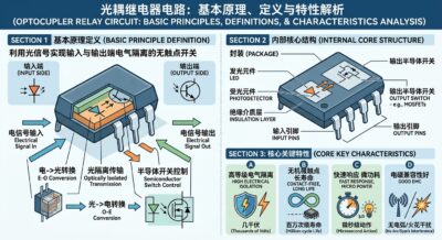
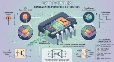
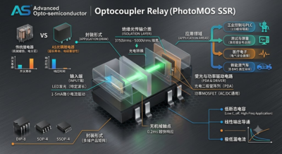
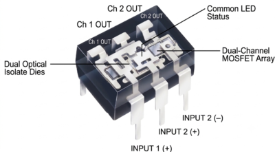
An optical relay is essentially a semiconductor power switch driven by photoelectric isolation technology. Its internal structure typically integrates three core modules:
**Input Stage (Light-Emitting Element):** Usually a high-performance infrared light-emitting diode (LED). When a control current is applied to the input, the LED emits an infrared light signal, achieving physical and electrical isolation between the low-voltage control side and the high-voltage output side.
**Intermediate Isolation and Photoelectric Conversion (Light-Receiving Element):** Comprises a photodiode array. The light signal passes through a transparent insulating medium to strike the array, which converts the light energy into voltage to drive the subsequent switching stage.
**Output Stage (Power Switching Element):** Utilizes a pair of back-to-back (series-connected) MOSFETs or a bidirectional thyristor (TRIAC). When the voltage generated by the photoelectric array is applied to the MOSFET gates, a conduction channel forms, enabling the switching (on/off) of the output load circuit.
Compared to traditional electromagnetic relays, optical relays eliminate mechanical wear and the risk of arc discharge while offering superior insulation and isolation capabilities. Compared to standard optocouplers, their output stage can directly handle bidirectional AC or DC voltages and features extremely low on-resistance.
**Analysis of Key Technical Specifications**
When designing circuits using optical relays, engineers must carefully evaluate the following key parameters:
**Off-State Voltage:** The maximum peak voltage the output stage can withstand in the off state. Adequate safety margins must be maintained for high-voltage power supplies or test equipment.
**On-Resistance:** The equivalent resistance of the output stage when in the conducting (on) state. On-resistance directly determines the heat generation and power loss of the relay during operation.
Photorelay Technology and Selection Strategies – Advanced Optical Semiconductors
Output-side parasitic capacitance: The parasitic capacitance between output pins when the switch is in the off state. When transmitting high-frequency signals or weak measurement signals, excessive parasitic capacitance can lead to signal leakage or coupling noise.
Isolation voltage: The maximum safe insulation voltage that the device can withstand between the input and output terminals.
Trigger current and operating time: The minimum current required to drive the input and the response speed of the switching action. The operating time of a photorelay is typically in the microsecond-to-millisecond range, far faster than the tens of milliseconds required for mechanical relays.
In photorelay chip design, the product of on-resistance and parasitic capacitance is a key figure of merit for chip performance. Lower on-resistance generally requires a larger die area, but this leads to a significant increase in parasitic capacitance. Therefore, optimizing the balance between these two factors for specific application scenarios represents a core technical challenge in optical semiconductor manufacturing.
Photorelay Classification and Selection Strategies
To achieve the optimal balance among performance, cost, and size, selection should be based on the priorities of the specific application scenario, following these classification-based matching strategies:
Low On-Resistance Type
Application scenarios: High-current control, power management, battery management systems, solenoid valve driving.
Selection priorities: Prioritize extremely low on-resistance and high continuous load current capability. Lower on-resistance effectively reduces conduction and thermal losses during high-current operation, ensuring the system can function without additional heat sinks.
Low Parasitic Capacitance Type
Application scenarios: Semiconductor test equipment, high-frequency signal switching, precision instrumentation, communication matrices.
Selection priorities: Focus on selecting products with ultra-low capacitance. Although the on-resistance of such products is relatively higher, they ensure extremely high attenuation and isolation for high-frequency AC signals in the off state, thereby preventing signal distortion.
Automotive-Grade and High-Insulation Type
Application scenarios: High-voltage power distribution units in battery electric vehicles (BEVs), insulation monitoring circuits, charging piles. Selection Criteria: Must meet automotive-grade quality certifications and satisfy stringent insulation withstand voltage standards and high-creepage-distance packaging requirements to withstand harsh operating conditions and high-humidity, high-temperature environments.
High-Speed Response Type
Application Scenarios: Pulse output for industrial controllers, high-speed data acquisition.
Selection Criteria: Evaluate microampere-level trigger currents and microsecond-level response speeds. Low trigger currents allow for direct driving by main control chip pins, eliminating the need for additional amplification circuitry.
Selection Evaluation Process and Engineering Considerations
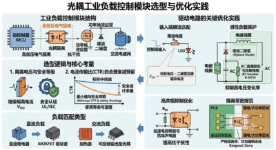
When implementing the design, the following process is recommended for final selection: First, determine the load type and voltage/current limits, selecting an off-state voltage that provides a safety margin. Second, evaluate signal frequency and loss requirements, balancing on-resistance against parasitic capacitance. Third, establish electrical isolation and environmental safety ratings, matching them with appropriate insulation withstand voltage specifications and automotive certifications. Finally, confirm package dimensions and thermal management, specifically assessing the heat dissipation capabilities of ultra-compact packages.
Engineering Design Tips:
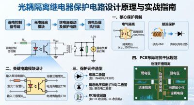
Input Drive Current Limiting: The input stage of an opto-relay consists of a light-emitting diode (LED) structure; a suitable current-limiting resistor must be connected in series during design to ensure the input current remains within the recommended range. This ensures reliable triggering while mitigating long-term degradation of the light-emitting component.
Overvoltage Protection: When driving inductive loads (such as relay coils or solenoid valves), the back electromotive force (back-EMF) generated during turn-off may exceed the off-state voltage limit. Consequently, a varistor or transient voltage suppressor (TVS) diode must be connected in parallel at the output for clamping protection.
As a product of the deep integration of microelectronics and optoelectronics, the opto-relay effectively resolves the issues associated with traditional mechanical switches—such as short lifespans and bulky sizes—as well as the high leakage current and poor isolation often found in standard solid-state relays. Driven by the adoption of high-voltage platforms in intelligent connected vehicles and the increasing precision required in semiconductor testing, miniaturized opto-relays—characterized by high density, multi-channel capabilities, and low loss—will continue to lead the technological trends in circuit isolation and signal switching. Mastering the precise alignment of system requirements with device parameters is key for modern hardware engineers to enhance product reliability and competitiveness. That concludes this article. If you found it helpful, please continue to follow our website at https://www.a-semi.com and our WeChat official account, “先进光半导体” (Advanced Opto-Semiconductor), for more news, information, and educational content.
Copyright Notice: Some content in our articles is sourced from the internet or user submissions. This website is responsible only for the compilation, formatting, and editing of the material. Such content is published to share information and does not imply endorsement of the views expressed or verification of the content’s accuracy. If any articles or reposted content raise copyright concerns, please contact us promptly so we can address the matter.