










主要产品
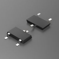
| Model | AHW-105A |
|---|---|
| Technology | InSb Hall |
| 工作电压 (V) | 1 |
| Maximum Input Current (mA) | 20 |
| Maximum Input Voltage (V) | 2 |
| VH[@1V@50mT] (mV) | 168~274 |
| Input Resistance (Ω) | 250~550 |
| VOS [@operating current] (mV) | -7 ~ +7 |
| 包装 | Ultra Thin SOT |
| Operating Temperature (°C) | -40 ~ 125 |
| Dimensions (mm) | 2.1*2.1*0.55 |
| 安装类型 | 表面贴装 |
| Packing | Tape & Reel |
| MPQ (Pcs) | 4000 |
Specifications & Application Scenarios
Specifications: The AHW-105A is an InSb Hall element in an Ultra-Thin SOT package, with a height of only 0.55mm. It operates at 20mA, delivering a Hall voltage of 168-274mV. It maintains the characteristic low InSb resistance (250-550Ω) and a ±7mV offset. It is rated for -40°C to 125°C.
Application Scenarios: The ultra-low profile is its defining feature. It is perfect for integration into extremely thin devices like smartphones, tablets, and ultrabooks for flip cover/hallpixel detection. It is also ideal for wafer-thin modules in credit card-sized devices, wearable health monitors, and flexible/printed electronics where z-height is a critical constraint, without sacrificing the inherent sensitivity of InSb technology.
Application Scenarios: The ultra-low profile is its defining feature. It is perfect for integration into extremely thin devices like smartphones, tablets, and ultrabooks for flip cover/hallpixel detection. It is also ideal for wafer-thin modules in credit card-sized devices, wearable health monitors, and flexible/printed electronics where z-height is a critical constraint, without sacrificing the inherent sensitivity of InSb technology.
相关产品
地 址:
中国深圳市福田区深南大道3003号北方工业大厦17层
电话:
+86-755-83-666-556
+86-755-83-666-557
+86-755-83-666-558
电子邮件:
apsemi@a-semi.com
sales@a-semi.com
design@a-semi.com
©2026 APSEMI co.,ltd